Previous Processing Updates

Screen printing electrical contacts to testing
April 21, 2022: We successfully completed an important milestone, transferring our process from a small university grade system to a much larger commercial system. This dramatically increased the size of our solar PV cells. Last week we completed our first working solar PV cell on the new system. We just electrically tested these devices with our solar simulator. Testing has shown good results and that the fabrication process has transferred to the new larger area equipment, while also identifying areas for improvement.
As part of the process, we screen printed electrical contact layers that you can see in the pictures above that allows us to test for uniformity across various areas of the cell.
The next step in our development is to continue to optimize the process to improve performance.

April 9, 2022, Larger area solar cells need electrical contacts to connect and deliver power. This shows a test of the screen-printed metal contact layer that we will be depositing on the solar cell. The next step in our development process is to deposit on a PV cell for electrical and solar testing.

March 2022, our team working diligently to fabricate and improve our solar materials. An important component of our technology is how we modify our materials’ semiconductor layers in order to achieve the desired properties. Here we are processing and evaluating some of our test materials.
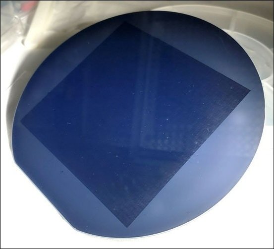
February 2022: The latest P4 solar cell materials prototype, much larger that we were fabricating just a few months ago. The 6-inch wide circular wafer contains a darker square, that is area treated with our proprietary materials’ process. This is one of the last precursor steps to building a completed (P4) solar cell.

In Dec 2021 -Jan 2022, we expanded our technical collaborations with a new development partner, another university in the US. We are excited that this new partnership provides us with additional prototype fabrication and testing capabilities, specifically for larger area prototypes and faster fabrication rate on commercial-grade equipment. This collaboration speeds up our technical development towards our commercialization goals.
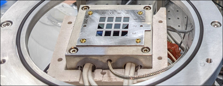
December 2021: A processing run where the same solar cell material is undergoing multi-variable tests under different conditions, including room temperature. The sample materials have a tracking grid, labeled with letters and numbers, with each sub-area under slightly different processing parameters. This allows us to track which set of fabrication conditions result in improved materials for each fabrication iteration.
This is a necessary part of taking our technology forward in materials development so that we can advance towards a commercial solution to bring a next-generation of solar PV to the world.

November 2021: These 9 squares show different processing conditions on a single wafer. We can tell that some of the squares look promising, while others, like the pale gray and white areas, were not the correct processing condition.
PI Energy’s technology enables a far lower energy use for fabrication of its non-toxic and stable solar PV materials. We have recently demonstrated one of the key processing steps at room temperature.
Many traditional solar PV modules are made using the Czochralski process at temperatures of over 1,400 °C (2,500 °F), the total process consumes about 11 kilowatt-hours (kWh) of energy per kilogram of silicon.
For PI Energy, the layers are not only far thinner, using less material, but also are formed at far lower temperature. A key material deposition process demonstration run in Nov.-Dec. 2021 was conducted at room temperature. We were expecting this process to be at low temperature, but were pleasantly surprised when we were able to successfully process the layer at room temperature. This is a big breakthrough for us since this benefits our final PV cell in several ways, including better performance of the cell layers, lower energy cost for production and enabling new low-cost flexible substrate materials that wouldn’t be available otherwise.

Making solar materials that can be installed on almost any surface, because they are lightweight, flexible, made of earth-abundant materials and non-toxic is only part of making PV globally scalable. It is important that the manufacturing of the PV cell should use a lot less energy, to lower costs and minimize the impact of the manufacturing process itself. That is the technology we are developing at PI Energy.

September 2021: An early, small P4 prototype. The blue regions are the PI Energy PV solar cell. This prototype measured an efficiency improvement of over 200% over the previous run, but still has a way to go!